|
| |

ISA Card-Edge Connector
The ISA card-edge connector is used to connect peripheral cards to the motherboard of
1980s and 1990s PCs, (before the advent of other interfaces and connectors, such as EISA, PCI, AGP, etc). The "ISA Connector" is actually two
card-edge connectors one 62-pin, one 36-pin. The 36-pin connector
(designated as having pins C1-D18) was added for 16-bit I/O at the time the IBM
PC/AT was developed.
Here's a look at an ISA card, showing the connector.
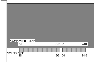
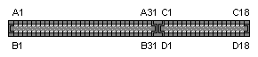
Here's what the ISA motherboard connector looks like:
| Pin |
Name |
Direction |
Description |
| A1 |
/I/O CH CK |
Card-to-PC |
I/O channel check; active low=parity error |
| A2 |
D7 |
Bidirectional |
Data bit 7 |
| A3 |
D6 |
Bidirectional |
Data bit 6 |
| A4 |
D5 |
Bidirectional |
Data bit 5 |
| A5 |
D4 |
Bidirectional |
Data bit 4 |
| A6 |
D3 |
Bidirectional |
Data bit 3 |
| A7 |
D2 |
Bidirectional |
Data bit 2 |
| A8 |
D1 |
Bidirectional |
Data bit 1 |
| A9 |
D0 |
Bidirectional |
Data bit 0 |
| A10 |
I/O CH RDY |
Card-to-PC |
I/O Channel ready, pulled low to lengthen memory cycles |
| A11 |
AEN |
PC-to-Card |
Address enable; active high when DMA controls bus |
| A12 |
A19 |
PC-to-Card |
Address bit 19 |
| A13 |
A18 |
PC-to-Card |
Address bit 18 |
| A14 |
A17 |
PC-to-Card |
Address bit 17 |
| A15 |
A16 |
PC-to-Card |
Address bit 16 |
| A16 |
A15 |
PC-to-Card |
Address bit 15 |
| A17 |
A14 |
PC-to-Card |
Address bit 14 |
| A18 |
A13 |
PC-to-Card |
Address bit 13 |
| A19 |
A12 |
PC-to-Card |
Address bit 12 |
| A20 |
A11 |
PC-to-Card |
Address bit 11 |
| A21 |
A10 |
PC-to-Card |
Address bit 10 |
| A22 |
A9 |
PC-to-Card |
Address bit 9 |
| A23 |
A8 |
PC-to-Card |
Address bit 8 |
| A24 |
A7 |
PC-to-Card |
Address bit 7 |
| A25 |
A6 |
PC-to-Card |
Address bit 6 |
| A26 |
A5 |
PC-to-Card |
Address bit 5 |
| A27 |
A4 |
PC-to-Card |
Address bit 4 |
| A28 |
A3 |
PC-to-Card |
Address bit 3 |
| A29 |
A2 |
PC-to-Card |
Address bit 2 |
| A30 |
A1 |
PC-to-Card |
Address bit 1 |
| A31 |
A0 |
PC-to-Card |
Address bit 0 |
| B1 |
GND |
N/A |
Ground |
| B2 |
RESET |
PC-to-Card |
Active high to reset or initialize system logic |
| B3 |
+5V |
|
+5 VDC |
| B4 |
IRQ2 |
Card-to-PC |
Interrupt Request 2 |
| B5 |
-5VDC |
PC-to-Card |
-5 VDC |
| B6 |
DRQ2 |
Card-to-PC |
DMA Request 2 |
| B7 |
-12VDC |
PC-to-Card |
-12 VDC |
| B8 |
/NOWS |
Card-to-PC |
No WaitState |
| B9 |
+12VDC |
PC-to-Card |
+12 VDC |
| B10 |
GND |
N/A |
Ground |
| B11 |
/SMEMW |
PC-to-Card |
System Memory Write |
| B12 |
/SMEMR |
PC-to-Card |
System Memory Read |
| B13 |
/IOW |
PC-to-Card |
I/O Write |
| B14 |
/IOR |
PC-to-Card |
I/O Read |
| B15 |
/DACK3 |
PC-to-Card |
DMA Acknowledge 3 |
| B16 |
DRQ3 |
Card-to-PC |
DMA Request 3 |
| B17 |
/DACK1 |
PC-to-Card |
DMA Acknowledge 1 |
| B18 |
DRQ1 |
Card-to-PC |
DMA Request 1 |
| B19 |
/REFRESH |
Bidirectional |
Refresh |
| B20 |
CLOCK |
PC-to-Card |
System Clock (67 ns, 8-8.33 MHz, 50% duty cycle) |
| B21 |
IRQ7 |
Card-to-PC |
Interrupt Request 7 |
| B22 |
IRQ6 |
Card-to-PC |
Interrupt Request 6 |
| B23 |
IRQ5 |
Card-to-PC |
Interrupt Request 5 |
| B24 |
IRQ4 |
Card-to-PC |
Interrupt Request 4 |
| B25 |
IRQ3 |
Card-to-PC |
Interrupt Request 3 |
| B26 |
/DACK2 |
PC-to-Card |
DMA Acknowledge 2 |
| B27 |
T/C |
PC-to-Card |
Terminal count; pulses high when DMA term. count reached |
| B28 |
ALE |
PC-to-Card |
Address Latch Enable |
| B29 |
+5V |
PC-to-Card |
+5 VDC |
| B30 |
OSC |
PC-to-Card |
High-speed Clock (70 ns, 14.31818 MHz, 50% duty cycle) |
| B31 |
GND |
N/A |
Ground |
| |
|
|
|
| C1 |
SBHE |
Bidirectional |
System bus high enable (data available on SD8-15) |
| C2 |
LA23 |
Bidirectional |
Address bit 23 |
| C3 |
LA22 |
Bidirectional |
Address bit 22 |
| C4 |
LA21 |
Bidirectional |
Address bit 21 |
| C5 |
LA20 |
Bidirectional |
Address bit 20 |
| C6 |
LA18 |
Bidirectional |
Address bit 19 |
| C7 |
LA17 |
Bidirectional |
Address bit 18 |
| C8 |
LA16 |
Bidirectional |
Address bit 17 |
| C9 |
/MEMR |
Bidirectional |
Memory Read (Active on all memory read cycles) |
| C10 |
/MEMW |
Bidirectional |
Memory Write (Active on all memory write cycles) |
| C11 |
SD08 |
Bidirectional |
Data bit 8 |
| C12 |
SD09 |
Bidirectional |
Data bit 9 |
| C13 |
SD10 |
Bidirectional |
Data bit 10 |
| C14 |
SD11 |
Bidirectional |
Data bit 11 |
| C15 |
SD12 |
Bidirectional |
Data bit 12 |
| C16 |
SD13 |
Bidirectional |
Data bit 13 |
| C17 |
SD14 |
Bidirectional |
Data bit 14 |
| C18 |
SD15 |
Bidirectional |
Data bit 15 |
| D1 |
/MEMCS16 |
Card-to-PC |
Memory 16-bit chip select (1 wait, 16-bit memory cycle) |
| D2 |
/IOCS16 |
Card-to-PC |
I/O 16-bit chip select (1 wait, 16-bit I/O cycle) |
| D3 |
IRQ10 |
Card-to-PC |
Interrupt Request 10 |
| D4 |
IRQ11 |
Card-to-PC |
Interrupt Request 11 |
| D5 |
IRQ12 |
Card-to-PC |
Interrupt Request 12 |
| D6 |
IRQ15 |
Card-to-PC |
Interrupt Request 15 |
| D7 |
IRQ14 |
Card-to-PC |
Interrupt Request 14 |
| D8 |
/DACK0 |
PC-to-Card |
DMA Acknowledge 0 |
| D9 |
DRQ0 |
Card-to-PC |
DMA Request 0 |
| D10 |
/DACK5 |
PC-to-Card |
DMA Acknowledge 5 |
| D11 |
DRQ5 |
Card-to-PC |
DMA Request 5 |
| D12 |
/DACK6 |
PC-to-Card |
DMA Acknowledge 6 |
| D13 |
DRQ6 |
Card-to-PC |
DMA Request 6 |
| D14 |
/DACK7 |
PC-to-Card |
DMA Acknowledge 7 |
| D15 |
DRQ7 |
Card-to-PC |
DMA Request 7 |
| D16 |
+5 V |
PC-to-Card |
|
| D17 |
/MASTER |
Card-to-PC |
Used with DRQ to gain control of system |
| D18 |
GND |
N/A |
Ground |
Note: B8 was /CARD SLCDTD on the XT ("card selected", activated by cards in XT's
slot J8)
|